Table Of Content

These are just some of the basic aspects a designer will need to excel in. As a designer becomes more experienced and familiar with the PCB design process, they tend to take on more of an engineering role and they become a critical part of product development. This includes circuit design and component selection, as well as placement in the PCB layout to ensure the final product will work as intended. Also note whether you'll be using any differential pair routing in the design.
EasyEDA – Best Browser-Based PCB Design Software
Any career path starts with education, especially in a technical area like PCB design. Today, PCB design is not something that is often taught formally in a university setting, and the level of quality in the instruction can vary across institutions. That being said, there are options for learning PCB design as part of an engineering degree, and there are industry-level courses designers can take to help them build their skill set.
PCB Layout
On top of that, it’s great for collaborating with mechanical teams thanks to its seamless integration with tools like Solidworks, Fusion 360, and PTC Creo, with every design change synced between programs. If you’re after the best overall PCB design software, few programs rival Altium Designer, but expect to pay for the pleasure. Breadboards are great for prototyping circuits, but they aren’t so good for actually using the thing you’re building.
Altium and IHS Markit Partner to Solve Component End-of-Life Issues for PCB Design - I-Connect007
Altium and IHS Markit Partner to Solve Component End-of-Life Issues for PCB Design.
Posted: Sat, 27 Apr 2024 09:20:18 GMT [source]
Learn How to Design PCBs with the Best PCB Design Tutorial
Prior to working in the PCB industry, he taught at Portland State University and conducted research on random laser theory, materials, and stability. His background in scientific research spans topics in nanoparticle lasers, electronic and optoelectronic semiconductor devices, environmental sensors, and stochastics. His work has been published in over a dozen peer-reviewed journals and conference proceedings, and he has written 2500+ technical articles on PCB design for a number of companies. He is a member of IEEE Photonics Society, IEEE Electronics Packaging Society, American Physical Society, and the Printed Circuit Engineering Association (PCEA). It's also important to annotate your schematics, as well as name nets when schematics get large and complex. As higher pin count devices are added to schematics, you can use net name assignments to keep things organized and easily track connectivity between components.
Step 2: Create a Blank PCB Layout
Back9 Design uses Solidwork's 3D CAD software platform for product designs. It also supports Pro-E and AutoCAD legacy projects, and uses Adobe Illustrator for graphic design requirements. To validate our work, we use a Design Rule Check (DRC), an area of electronic design automation. We also do schematic and circuit board modeling using specialized software.
PCB Design and Layout Services
PCB Design Review: DPI-LVDS Sony Vaio LCD Devboard - Hackaday
PCB Design Review: DPI-LVDS Sony Vaio LCD Devboard.
Posted: Tue, 12 Mar 2024 07:00:00 GMT [source]
He studied electrical engineering, emphasizing computer architecture and hardware/software design at the University of Southern California. As an embedded software engineer in the aerospace industry, his focus on firmware development and data acquisition for auxiliary power units highlighted the importance of cross-functional collaboration. Through his engineering experiences, he discovered his passion for enabling cross-discipline engineers to communicate effectively.
Unique Features and Services of EasyEDA
Then, we create a technical specification and set a budget and deadlines. To this day, I’m still surprised at the number of new designers that hesitate to place a ground plane in their PCB stackup. Many basic noise problems that affect digital and analog signals can be traced back to the absence of a ground plane in the device. In modern PCBs, it is a standard guideline to use a solid ground plane throughout your device. There are some exceptions where split planes or a star ground on a PCB are appropriate, but those approaches are not appropriate for the vast majority of digital and analog designs. For more circuit guides and other electrical engineering posts, check out the other articles on The Engineers Post.
SUPPORT
Check out other Getting Started guides for insight into using robust features like Draftsman® and ActiveRoute®. The Gerber X2 file will be immediately loaded into the Altium Designer viewing tool, CAMtastic. Alternatively, batch output files can be rapidly generated, so that the PCB can be fabricated with Output Job Files.
It will also help if you ever need to debug the board while testing. You can also add a company logo and part numbers using the image tools and text tools in the PCB Editor. These elements need to be placed in the Top Overlay or Bottom Overlay layers in the PCB layout. If you’re working on a high speed/high frequency circuit board design, you can use the built-in impedance profiler to ensure impedance control in your board. The impedance profile tool uses an integrated electromagnetic field solver from Simberian to tailor the geometry of your traces to meet a target impedance value.
Back9 also has extensive programmable logic experience to support your complicated designs. In the past, PCB design was something you could pick up actively because it was something of a trade and there was a focus on drafting with scale drawings or models. Today, because the required breadth and depth of skills has increased significantly, it is recommended that PCB designers obtain an electrical engineering degree, or possibly a computer engineering degree. If you want to work in manufacturing or process development, a degree in materials science or chemistry is recommended. This will give designers access to a broad range of skills that are demanded in the modern PCB design job description. As electronics moved from vacuum tubes and relays to silicon and integrated circuits, the size and cost of electronic components began to decrease.
For example, the 3D renderings offered by professional solutions like Altium are considerably higher quality than those you get in free programs. Another benefit of OrCAD is the dynamic differential pair routing, which makes it easy to meet length and phase pin-to-pin constraints because traces can bend without causing any electrical issues. You can switch between 2D and 3D in this software’s highly intuitive and interactive environment, allowing you to examine each aspect of your layouts.
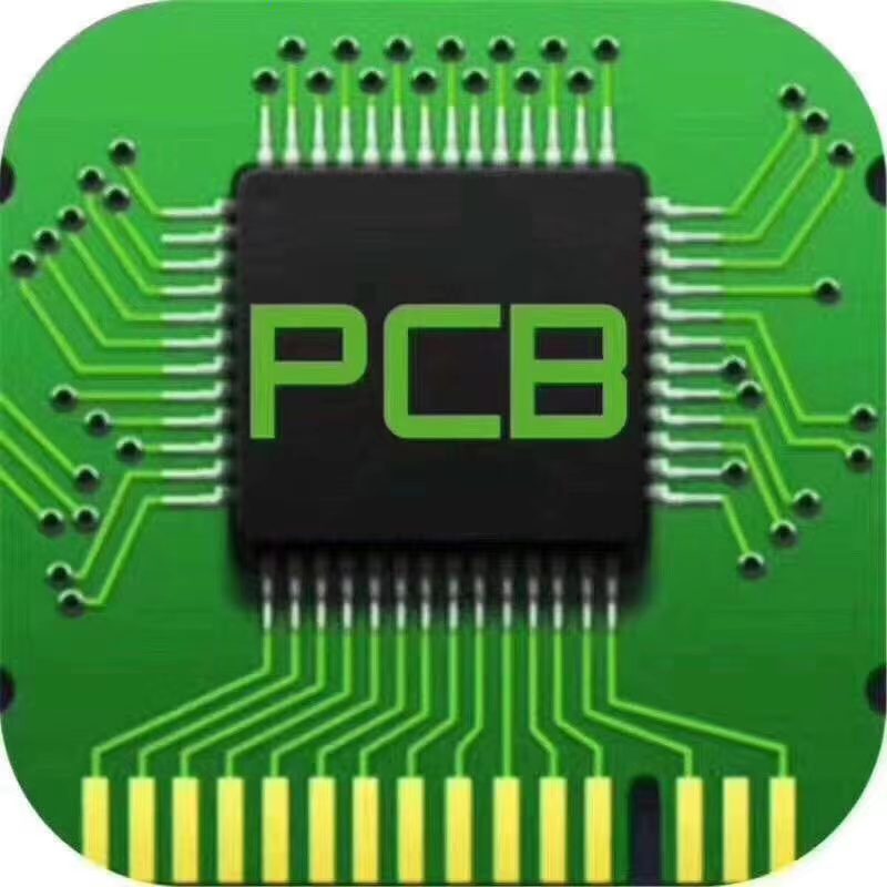
On the basis of these data, we can estimate how much it will cost to produce the required number of devices. If you don’t have a specification yet, we will be happy to prepare it for you. It is a board that has lines and pads that connect various points together. In the picture above, there are traces that electrically connect the various connectors and components to each other. A PCB allows signals and power to be routed between physical devices.


No comments:
Post a Comment